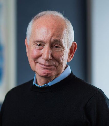
Lionel C. Kimerling
Primary Impact, Materials, Research Type
Contact Info
Assistant
Research
Professor Lionel Kimerling’s research centers on the design and processing of semiconductor materials and devices. His work has had a fundamental impact on the understanding of chemical and electrical properties of defects in semiconductors. His research teams have enabled long-lasting telecommunications lasers; produced the first 1 MB DRAM, or dynamic random-access memory; developed semiconductor diagnostic methods; and pioneered silicon microphotonics. His MIT research on silicon processing has addressed integrated circuit fabrication, microphotonic materials and devices, solar energy conversion, and environmentally benign integrated circuit manufacturing.
Biography
Professor Kimerling earned a BS in metallurgy in 1965 and a PhD in 1968, both from MIT. Before joining the DMSE faculty in 1990, he headed the Materials Physics Research Department at AT&T Bell Laboratories.
Kimerling was the founding director of the MIT Microphotonics Center and served as director of the MIT Materials Processing Center for 15 years, establishing the organization as the industry portal for faculty across all materials-related disciplines. He is the lead for MIT’s Initiative for Knowledge and Innovation in Manufacturing and served as the AIM Photonics Institute founding executive for education and workforce development.
He has authored more than 600 technical articles and holds more than 100 patents in integrated photonics and semiconductor processing. He served as the 1994 President of The Minerals, Metals & Materials Society (TMS). He is a Fellow of the University of Tokyo School of Engineering and numerous professional organizations, including TMS, the Materials Research Society, the American Physical Society, the American Association for the Advancement of Science, and Optica.