March 4, 2026
Stacking 2D materials for more capable chips
At a Nature Conference in Beijing, Professor Jeehwan Kim showcased his breakthrough in layered 2D semiconductors.
Categories:
In the Media, Computing and Data Science
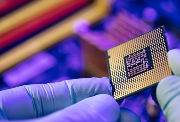
Professor Jeehwan Kim grows alternating layers of 2D materials without a silicon wafer.
Credit: Shutterstock
At the Nature Conference on “Novel Materials and Devices for the Post-Moore Era,” 20 speakers and more than 300 researchers from around the world explored the limits of silicon-based transistors and new materials for next-generation computing. Professor Jeehwan Kim of MIT’s Departments of Mechanical Engineering and Materials Science and Engineering described how his team can grow alternating layers of 2D materials directly atop one another—bypassing silicon wafers. “It means we can now add more functions to semiconductors,” Kim explained.
Watch Kim discuss his work in a new video, and read the full story in Nature Portfolio.
Related Stories