From Dislocations to Luminescence: Epitaxial Strategies for Infrared Optoelectronics

Speaker
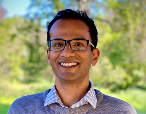
Kunal Mukherjee
Assistant Professor of Materials Science and Engineering, Stanford University
About This Talk
Integrating dissimilar semiconductors on a single crystalline platform could enable the next generation of devices for optical communication and sensing. Materials such as III–V and IV–VI semiconductors, when epitaxially grown on silicon, offer distinct optoelectronic properties that expand the capabilities of this scalable system. However, bridging the structural and chemical mismatches between these crystals while minimizing defect generation remains a significant materials science challenge.
In this talk, Stanford University’s Kunal Mukherjee will present new insights into how dislocations arising from integration severely limit the performance of III-V telecom lasers. He will then show how his group employed alloy hardening and quantum dots to realize dislocation tolerant lasers grown on silicon. Building on lessons from III–V integration, Mukherjee will highlight emerging opportunities in IV–VI semiconductors such as PbSe–SnSe, which are inherently more tolerant of defects, enabling efficient mid-infrared light emission for sensing applications. He will also discuss efforts to engineer crystalline–crystalline phase transitions in these semiconductors for reconfigurable photonic circuits. By advancing the understanding of crystal defects in mismatched epitaxy, his work identifies new pathways for scalable integration of optoelectronic materials.
About the Speaker
Kunal Mukherjee is an assistant professor in the Department of Materials Science and Engineering at Stanford University. His research focuses on compound semiconductor thin film synthesis and defect science. He received a BEng in electrical engineering from Nanyang Technological University, an MS from the National University of Singapore, and an MEng and PhD in materials science and engineering from MIT. Before joining Stanford, he served as an assistant professor in the materials science department at UC Santa Barbara (2016-2020) and held postdoctoral appointments at IBM and MIT. His work on epitaxy and crystal defects has been recognized with an National Science Foundation CAREER award, the Corbett Prize at the International Conference on Defects in Semiconductors, the Young Scientist Award at the International Symposium on Compound Semiconductors, and the Young Investigator Award at the North American Molecular Beam Epitaxy conference.
About the MSE Seminar Series
The Materials Science and Engineering (MSE) Seminar Series features distinguished speakers from leading institutions, offering a platform for sharing groundbreaking research, innovative ideas, and entrepreneurial experiences. Held multiple times each semester, these seminars bring global perspectives world to MIT’s materials research community, exposing students, faculty, and postdocs to cutting-edge concepts and valuable networking opportunities.