Listening to the body’s language
Growing up in Colombia, Diana Grass had a simple response whenever someone told her something was impossible.
“I’ll figure it out.”
It’s a phrase that she still lives by today as PhD candidate in the Harvard-MIT Program in Health Sciences and Technology (HST), as she develops soft bioelectronic devices to study the physiological signals through which the brain and body communicate.
“I’ve always been fascinated by one question: How do complex systems work?” Grass says.
An instinct to get to the bottom of things has guided Grass’ unconventional academic journey across continents and disciplines. Before becoming a neuroscientist and engineer, Grass studied philology and education to understand how language evolves, preserves knowledge, and shapes human communication. Looking back, she sees a common thread. “I wasn’t just studying language,” she says. “I was learning how complex systems communicate.”
But it wasn’t until she moved to the United States and began working as a medical interpreter that her scientific interests took a new direction.
“Every day, I translated conversations between physicians and patients with neurological disorders,” she says. “Watching those interactions sparked a fascination with the brain. I was intrigued by how a single organ could shape how we communicate, and ultimately who we are.”
Working alongside clinicians, Grass watched them rely on laboratory tests, medical imaging, and vital signs to understand what was happening inside the body. Despite remarkable advances in medical imaging and diagnostics, clinicians still rely largely on isolated snapshots of biological processes that are continuously changing inside the body.
“The body is communicating all the time,” she says. “We still lack the tools to understand its language.”
Determined to better understand the brain, Grass returned to school to study neuroscience with a minor in pre-medicine. She joined an immunology laboratory at Rutgers New Jersey Medical School, where she investigated neuroimmune communication and gained a new appreciation for the body’s interconnected physiology.
“Until then, I had been fascinated by the brain,” she says. “My work in immunology made me realize that the nervous system doesn’t function in isolation,” she says. “It continuously communicates with the immune system and peripheral organs to coordinate physiology and maintain homeostasis. To understand health and disease, we have to understand how those interactions preserve or disrupt that balance.”
That realization transformed her scientific focus from understanding the brain to understanding how the nervous system coordinates physiology through continuous communication with the rest of the body, beginning with the immune system.
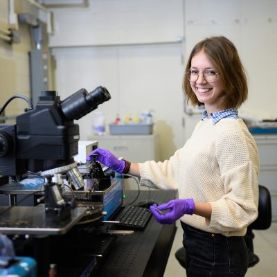
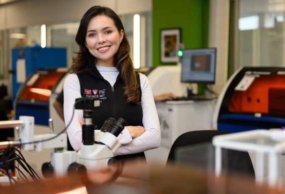
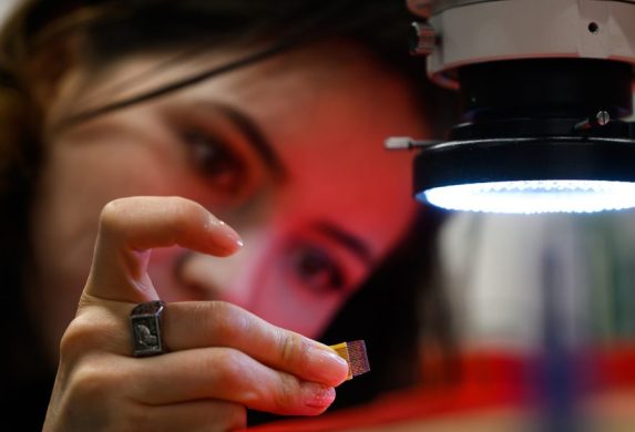
The complexity of that question ultimately brought Grass to pursue a PhD in medical engineering and medical physics with the HST program. She works in the Bioelectronics Group, led by Polina Anikeeva, the Matoula S. Salapatas Professor and head of MIT’s Department of Materials Science and Engineering. Grass also uses facilities in the T.J. Rodgers Laboratory and MIT.nano, and is part of the K. Lisa Yang Brain Body Center.
Today, Grass develops soft bioelectronic devices that integrate seamlessly with soft peripheral tissues without damaging them, to continuously monitor multiple physiological signals while enabling electrical recording and stimulation of neural circuits. These technologies provide a new way to investigate how neural communication coordinates physiology across the entire body. This knowledge could enable earlier diagnosis, more precise therapies, and a new generation of bioelectronic medicine.
For Grass, the work has taken on an even deeper significance since becoming a mother. Grass has two school-age children and for her, the possibility of developing technologies that help detect disease earlier and personalize treatments isn’t just a scientific goal; it’s one she hopes will shape the future of medicine for the next generation.
“I want to contribute to a future where medicine understands the body physiology well enough to predict disease instead of simply reacting to it, personalize therapies with greater precision, and ultimately give families more healthy years together,” she says. “Because once you become a parent, every scientific question becomes deeply human.”
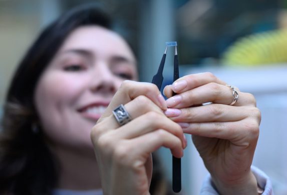
The complexity of Grass’ research has required her to step well beyond her original training. After studying neuroscience and immunology, she immersed herself in materials science, systems physiology, device fabrication, bioelectronics, and surgery to develop the tools needed to answer fundamental biological questions.
“The scientific question was bigger than any one discipline,” she says. “HST taught me to begin with biology, not disciplines. Once you understand the biological principles, medicine, engineering, and science stop being separate fields. They become complementary ways of answering the same question.”
The constant need to learn a new discipline has been both the most rewarding and challenging part of Grass’ research so far.
“Every time I crossed into a new discipline, I felt like an immigrant again,” she says. “I had to learn a new language, understand a new culture, and earn the trust of people who had spent their careers there.”
Grass’ passion for understanding cultures extends well beyond the lab. Soon after arriving at MIT, she co-founded the Graduate First-Generation Low-Income Student Group to create a supportive space for students and connect them with the resources they need to thrive. What began as a small initiative has grown into a community of more than 300 graduate students representing over 60 countries, connecting students with faculty, alumni, entrepreneurs, and industry leaders.
“It has been really rewarding to see new GFLI leaders emerge and continue this legacy,” Grass says.
As an avid traveler, Grass’ favorite pastime is exploring new cultures, whether that be through learning a new traditional recipe or a new language. She speaks four languages fluently and can say “thank you” in roughly 50 more.
Whether she’s cooking Thai food with her children or introducing friends to recipes from around the world, she sees food as another language capable of connecting people across cultures. That same philosophy shapes how she thinks about science.
“I’ve realized that every culture has its own language and every scientific discipline its own way of understanding the world,” she says. “Looking back, every stage of my life has been about understanding how complex systems communicate. Today, my goal is to help medicine understand the principles that govern communication across the human body in health and disease.”
Related Stories